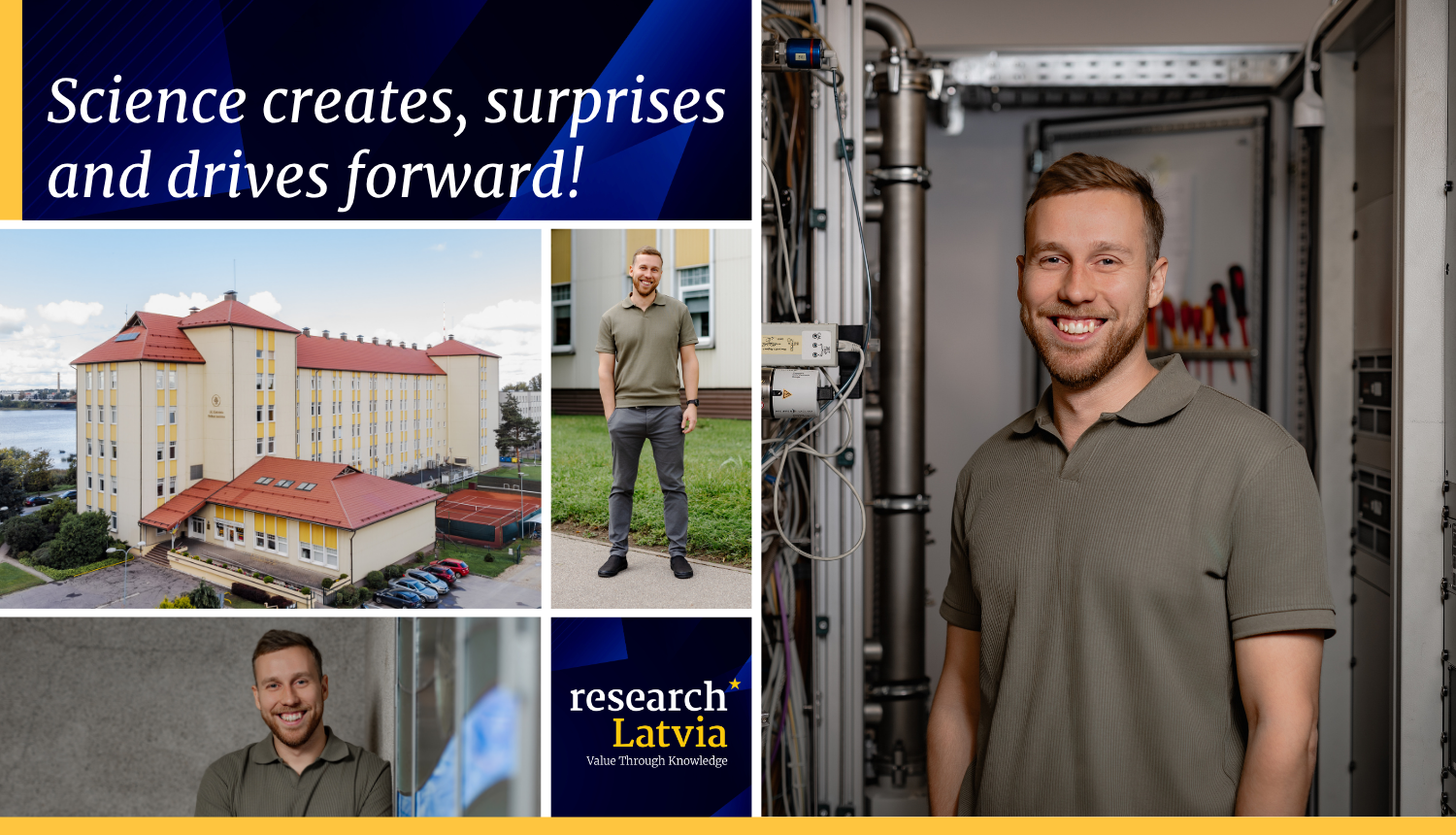
Lead researcher at the Thin Films Laboratory of the Institute of Solid State Physics, University of Latvia (UL ISSP) and head of the Semiconductor Thin Film Nanotechnology Group, PhD Edgars Butanovs focuses on developing ultra-wide bandgap semiconductor coatings – materials with the potential to transform high-power electronics and next-generation energy systems. His research explores how these advanced thin films can improve efficiency, reduce losses and enable new applications in optoelectronics, sensing and renewable technologies.
“Research and development of new materials are often the first steps towards innovation in high-tech industries. As a researcher, I feel pleased when discoveries at the atomic level lead to tangible results on a global scale.”

UL ISSP is one of the leading materials science and interdisciplinary research centres in the Baltic Sea region, generating new knowledge and promoting both scientific excellence and practical technological development. The Institute’s research areas range from advanced functional materials and nanostructures to photonics, energy solutions, and high‑quality thin‑film coatings.
At the Thin Films Laboratory, Edgars studies innovative materials that can be used in optoelectronics, sensing technologies and energy applications. His work pays particular attention to ultra‑wide bandgap semiconductor coatings. These materials could make high‑power electronics significantly more efficient by reducing energy losses in electric vehicles, renewable energy systems such as solar and wind power plants, and future smart grids. As electrification accelerates, the need for efficient, flexible and secure energy distribution systems becomes increasingly critical. New semiconductor materials could enable next‑generation high‑power devices that help save substantial amounts of energy simply through more efficient conversion.
Ultra‑wide bandgap semiconductors also have important applications in developing compact far‑ultraviolet detectors. These detectors can be used for monitoring corona discharge in electrical networks, studying the ozone layer, early forest fire detection, space science and defence technologies.
Edgars emphasises that while Latvia cannot compete with the world’s semiconductor giants in terms of investment and scale, Latvian scientists can still develop technologies that address important societal challenges. He welcomes the rapid growth of science‑intensive start‑ups in Latvia, which can transform laboratory innovations into unique products – such as optical sensors for the space industry or dual‑use applications.
Alongside applied research, Edgars is committed to advancing fundamental research. He studies the synthesis and physical properties of nanomaterials, such as nanowires, that provide insights into how matter behaves at near‑atomic dimensions. These fundamental studies, often supported by national research programmes, form the essential groundwork for future breakthroughs and new technologies. Despite their long‑term nature, such projects are crucial for enabling Latvian laboratories to generate new ideas instead of merely refining existing technologies.
Edgars’ work shows how targeted research, ranging from atomic‑scale discoveries to real‑world applications, can drive innovation not only within Latvia but also on the global stage.
The science calendar “Research Latvia 2026” and the researcher descriptions were developed within the ERDF-funded project No. http://1.1.1.1/1/24/I/001 “More Efficient Implementation and Management of Latvia‘s Science Policy”, implemented by the Ministry of Education and Science.